Advanced ultrafast laser processes for consumer electronics and semiconductor manufacturing — SiC wafer dicing, brittle-material cutting, laser slotting, micro-nano structuring and coating removal.
Ultrafast picosecond/femtosecond laser processes engineered for the hardest problems in 3C and semiconductor production.
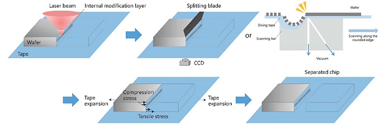
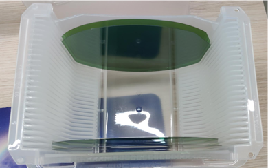
Laser stealth cutting of silicon carbide wafers for semiconductor production — internal modification followed by clean tape-expansion separation.
Kerr-effect self-focusing forms a ~1μm filament through glass and transparent materials — burst-mode cutting with pristine cross-sections.
Innovative laser direct-writing photoresist technology replaces photolithography masks — fast, flexible PCB sample preparation.
Cutting aluminium nitride and ceramic substrates of different thicknesses, plus SiC rod cutting and wafer hard punching.
Galvanometer scanner with F-Theta optics delivers precise micro-slots — profile-verified to μm-level depth accuracy.
Surface texturing of stainless steel, zirconium, titanium and aluminium for functional and cosmetic finishes.
Selective PVD coating removal and ceramic surface laser heat-treatment discoloration — no masks, no chemicals.
Diffractive optical elements transform Gaussian spots into flat-top beams for uniform energy distribution across the work area.
Laser cleaning of silicon carbide material surfaces — contamination removal without contact or abrasives.
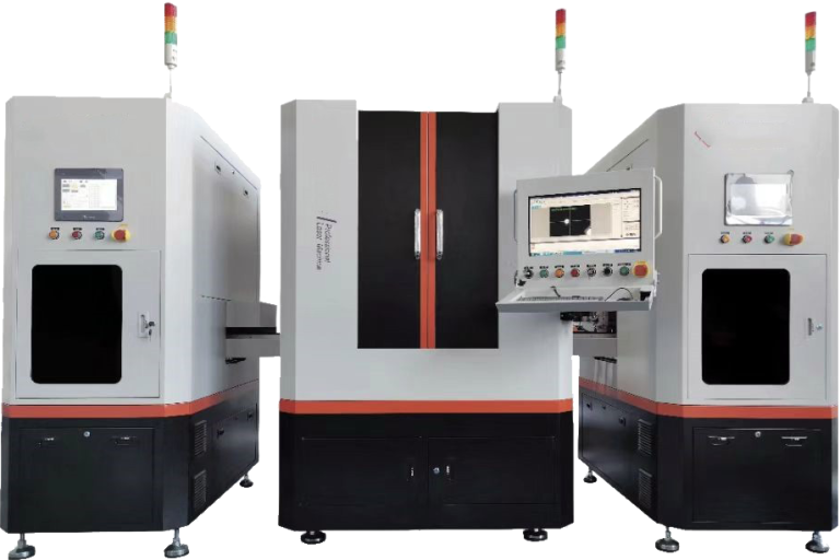
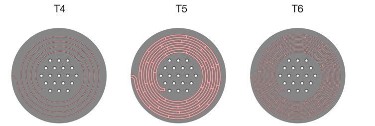
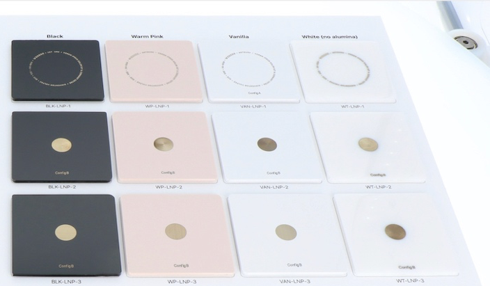
Precision marking, welding and cutting — earphone solder ball soldering, VR 3D surface marking, wearable glass cutting, back-cover deep engraving, groove marks and accessory marking.
Batteries, motors and automotive electronics — metal and dissimilar-metal welding, high-power welding, busbar and cell-tab joining.
Wafer marking and dicing, IC marking, plasma cleaning and AOI inspection support — including PCB/FPCB precision cutting.
Barcodes, data matrix and 3D marking for food, medical and tobacco packaging — permanent, high-speed traceability coding.
Wafer dicing, glass cutting, slotting or structuring — tell us your material and specification, and we'll arrange process trials.
